Printed circuit boards are widely recognized for their essential role in electronics tech, but I think they have underappreciated potential as an artistic medium too. The PCB badge projects you see at hacker conferences always catch my eye for their unique look and creativity.
For a prime example, check out the world’s thinnest boombox PCB. Incredible work, 10 out of 10, love it!

It’s probably fair to say that PCB art has an inflated cool-factor in my mind due to my inability to make such things for so long!
Back in 2017 I struggled with electronic-CAD software for a sumo robot project, and ever since I’ve found excuses & clever ways to avoid trying again. I’ve leaned on friends with the skillset. I’ve used off the shelf electronics when I probably shouldn’t have. Anything to avoid that infuriating buggy nonsense! (I have strong opinions about software usability OK?!)
Well, things have changed. My patience muscle is infinitely stronger with children in my life, but the tools have definitely gotten better too. Somewhere along the line KiCad’s open source PCB design software evolved from intolerable into something I enjoy using.
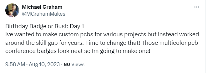
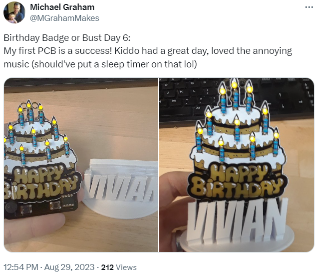
Last August I decided it was time to work through this skill limitation. I set a goal for myself to produce a birthday cake badge in time for my daughter’s 7th birthday at the end of the month!
In this post I’ll share some practical tips I picked up along the way plus a new product reveal!
Step 0: Make a public declaration so you cant back out 😛
Step 1: Prototype Circuit Design
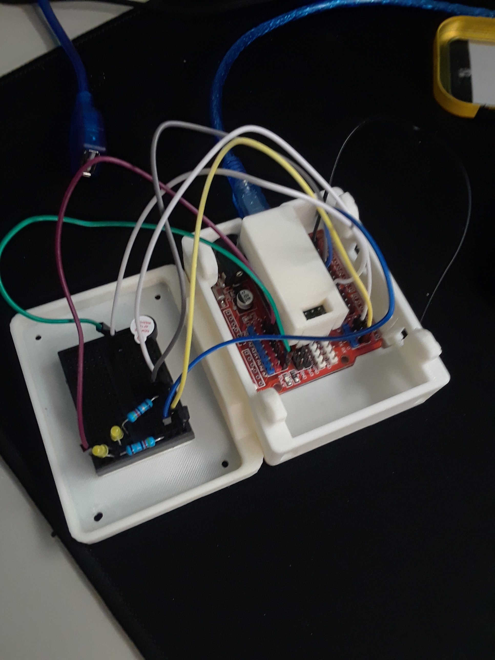
I made a quick sketch & prototyped it out with parts I had on hand to check my initial assumptions.
I decided to use an ATTINY85 & through-hole components to make it easy. The Tiny only has 5 IO pins, & a 40ma/pin limit, so I had to use a transistor to drive the LEDs. Apparently I wired them in a way they’re not meant to be used which made troubleshooting really fun. But somehow it ended up working out anyway. I did some shopping & price comparison then ordered enough for 10 badges from Amazon.
Useful Tool: Calculate resistor size for an LED
Useful-er Tool: Simulate IOT Circuits & Code in your browser

Step 2: KiCad Circuit Schematic
The software will let you get away with assigning any attributes (or none at all) to a symbol, but don’t be tempted to take shortcuts here because it will hurt later. Take time to make sure every component has an appropriate symbol that matches it’s actual function (i.e. use a switch symbol with exact same number of ports as the real switch).
Make sure every component has a linked footprint that looks exactly the way you want it to look before proceeding. You can copy footprints to make custom ones. The default footprint library is small, you’ll need to import some libraries from your favorite electronics suppliers:
- https://www.kicad.org/libraries/download/
- https://github.com/adafruit/Adafruit-Eagle-Library
- https://www.digikey.com/en/resources/design-tools/kicad
- https://github.com/sparkfun/SparkFun-KiCad-Libraries
When you’re done schematizing export the netlist for later. (File>Export>Netlist. It’s a tabular list of every connection).

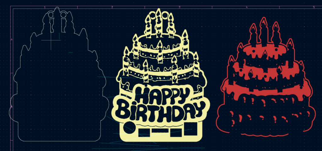
Step 3: PCB Concept Art
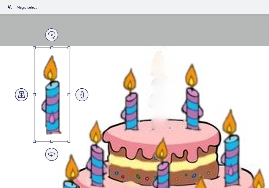
I found an image I liked online, & used Microsoft “Paint 3D” to cut & paste components within the image. The ‘magic select’ tool is super useful, it even tried to backfill the empty space behind the candle when I cut it out! (PowerPoint can do this too.)

Step 4: Vectorize the Image
You need an SVG that’s properly layered to be able to use it in KiCad. I tried Inkscape’s trace-bitmap function, but it wouldn’t do the job because the cake image was too pixelated & had too many colors.
So I uploaded the cake bitmap image to https://vectorizer.ai which perfectly cleaned & grouped everything together into an svg. A critical part of this process, that tool is currently pseudo-free & did an incredible job.

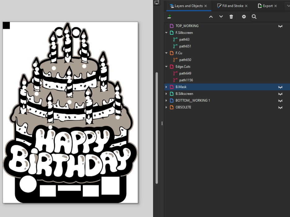
Step 5: Arrange the SVG Layers
This step is the meat of the manual work. Bring that clean SVG into Inkscape & get down to business consolidating colors & organizing layers. You need a separate layer for each color and the edges of the board. You’ll have to get creative with your use of color because you can only get up to 4 unique colors on a standard board, like this:
- Bare stripped board (FR4). The only color choice is translucent amber. (it is UV reactive though)
- Exposed traces. Color choices are shiny tin or gold coated copper for extra $.
- Solder Mask. Color choices are green, white, black, blue, yellow, red, & purple. (Some but not many, manufacturers will offer a second color of solder mask for extra $.)
- Silkscreen. Color choices are white or black.
One thing I didn’t realize on my first try is that solder mask is automatically applied to your entire board, so the layer you make in Inkscape needs to indicate everywhere you DON’T want solder mask. Also, silkscreen can only be applied over the top of solder mask. It’s ink, it wont stick to anything else.
Cutting, pasting, recoloring, combining shapes…this step is a lot of work, but I enjoy it. The first one took longer than I hoped but it was entirely a skill issue. I’ve done it enough times now I can wrap it up in a couple hours.
Hot tip: You have to ungroup shapes all the way, convert objects & strokes to paths, then combine them into a single path for each layer. (Otherwise multiple objects/paths within a layer will import with offsets into KiCad.)
Hotter tip: Add a tiny square in the top left at position 0,0 for every layer, this will keep them aligned in KiCad.
Hottest Tip: Set your stroke width for everything to be the same. Something small & round like 0.1mm. (metrically ’round’ anyway) The stroke width is considered an inclusive part of the shape in KiCad & varying widths will cause a slight misalignment that will rive you crazy!
I was worried about a potential design error and finishing on time for her birthday so I experimented with a custom sticker as a layover on the PCB. The end result could’ve been made to work but the edges were hard to line up & the sticker colors don’t look nearly as good as solder mask & silkscreen colors. The useful lesson here is printing your image onto paper 1:1 does make for a nice mock up.
This is what my layers looked like in Inkscape. From here you use the batch export tool to export these as separate SVG’s.


Step 6: Import the SVG Layers into KiCad Board Editor
This step is only possible recently. You used to have to use weird diy Inkscape extensions like ‘svg2Shenzen’ from abandoned GitHub repositories.
Now its just File>Import>Graphics & select which layer you want the graphic on. Use the little squares to keep them aligned & drag them to the center of the page to do your layout.
Then click File>Import>Netlist & find that file we made in the KiCad Schematic editor. Poof, all of your component footprints appear along with phantom lines telling you where they need to connect. The rest is just connecting the dots! I don’t mind this task but there are new AI tools out there for this phase which probably make sense if you have >2 layer boards and hundreds of connections. (Quilter & Flux.ai)
Hot Tip: There is not currently a way to link a graphic to your netlist, so the decorative exposed copper cannot have a functional use!
If a component doesn’t line up with the cutouts you allocated for it, its tempting to edit the graphic directly in KiCad. But you’ll find it tedious work since curves are converted into hundreds of tiny segments on import. Best to adjust in Inkscape and reimport.

Step7: Order PCBs.
Run that design rule checker then ship it out. Electronic components, including PCBs, are insanely cheap so in this market your real cost is time since it takes 2-3 weeks from the day you order to arrive in your mailbox (unless you expedite it, which I did for the birthday cake).
Best I can tell is Chinese board houses subsidize small orders & hope to earn big profitable orders from you. If you can find a special going on then even shipping will be discounted. Look at the deals I got below: 5 custom boards for $3.50 total. Blows my mind.
Hot Tip: PCB fab price comparison. I like JLCPCB, and they have a dedicated coupon page here.

Step 8: Assemble & Accessorize
Since the design file was an SVG you can import it into TinkerCad and make a 3d model of it. While I waited for shipping I made a fun little stand to use it as a cake topper. Everything arrived just in time for the big day!
Step 9: PCB ALL THE THINGS!
By this point I’m hooked. 1st project a success. Cheaper and more doable on a short schedule than expected. And the properties of PCB based products are exactly what I’m looking for to grow my small business. Lots of potential here!
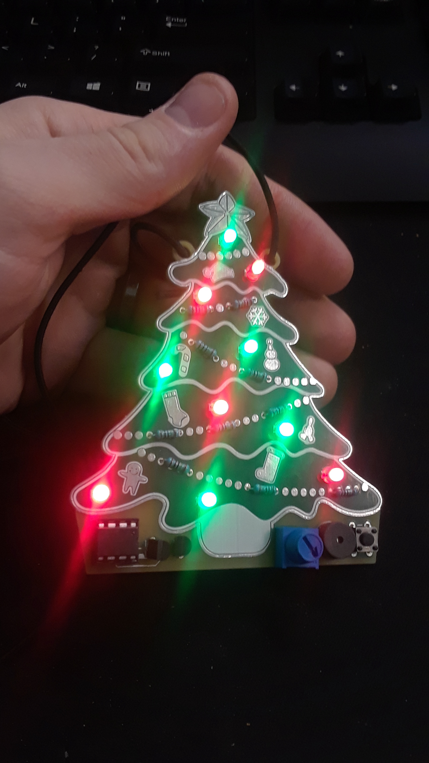
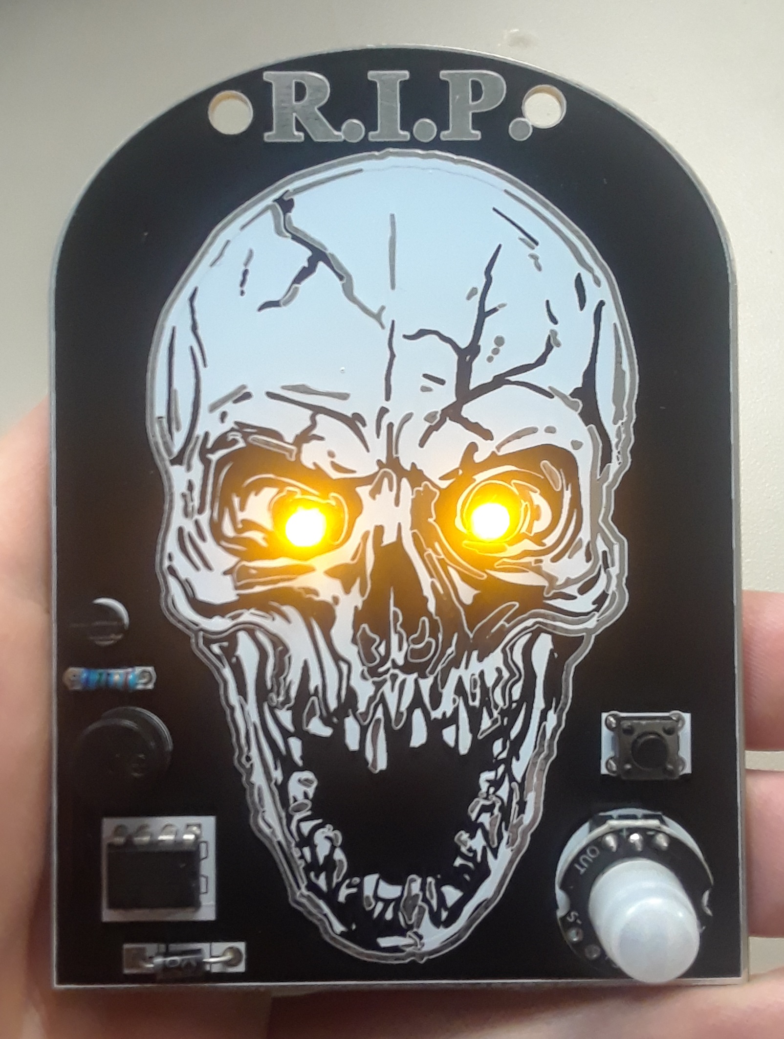
I’d thought it’d be fun to experiment more so I went ahead and designed a set of holiday themed badges. This story has been a few months in the making so you get to see what I came up with!
I ran into some interesting challenges along the way:
The options for powering these small devices from batteries is surprisingly not straight forward.
ATTINY runs on 2.7v to 5.5V. I could have used 2-3 AA batteries but the battery packs have much larger dimensions than the badge. LiPo pouch batteries are small and the perfect voltage range but I didn’t want to integrate a battery management system on the badge to keep it simple.
A stand alone CR2032 coin cell holder was exactly what I wanted in theory. Clean, flat, simple. In practice I found they cause sporadic instability unless you have a decoupling capacitor to smooth out their voltage. At 3V each, I was surprised to find that 1 coin cell would do the job albeit with diminished brightness & life. Having 2 coin cells is theoretically 6V and above my usable range BUT the load causes that voltage to sag into the acceptable range for the Tiny & the LEDs. Hacky & not 100% stable voltage, but it does work.
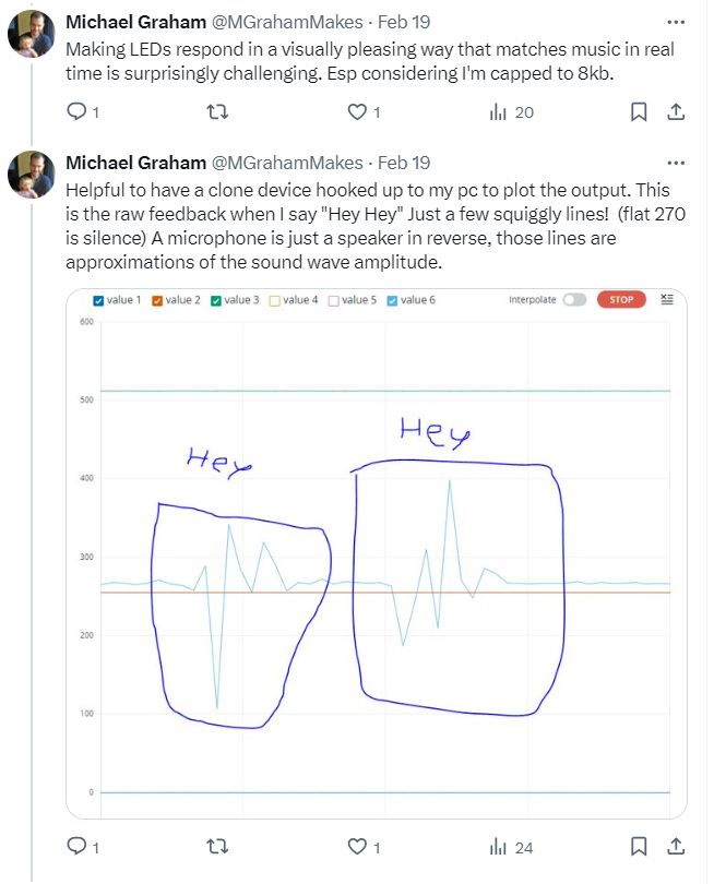
I also found a neat AAA to 5V boost converter module, and I love the simplicity it offers. Still it’s limited to 200ma max which wasn’t enough to drive the St Patty’s Day Booze-O-Meter novelty breathalyzer. (Also running the screen on just 8kb of memory is a big limitation.)
The other thing I learned is that the ATTINY may use the Arduino IDE, but the hardware & software both have notable limitations that Arduino does not. The system will compile without errors, then fail on runtime without giving you feedback if you surpass these limits! Super fun to troubleshoot.
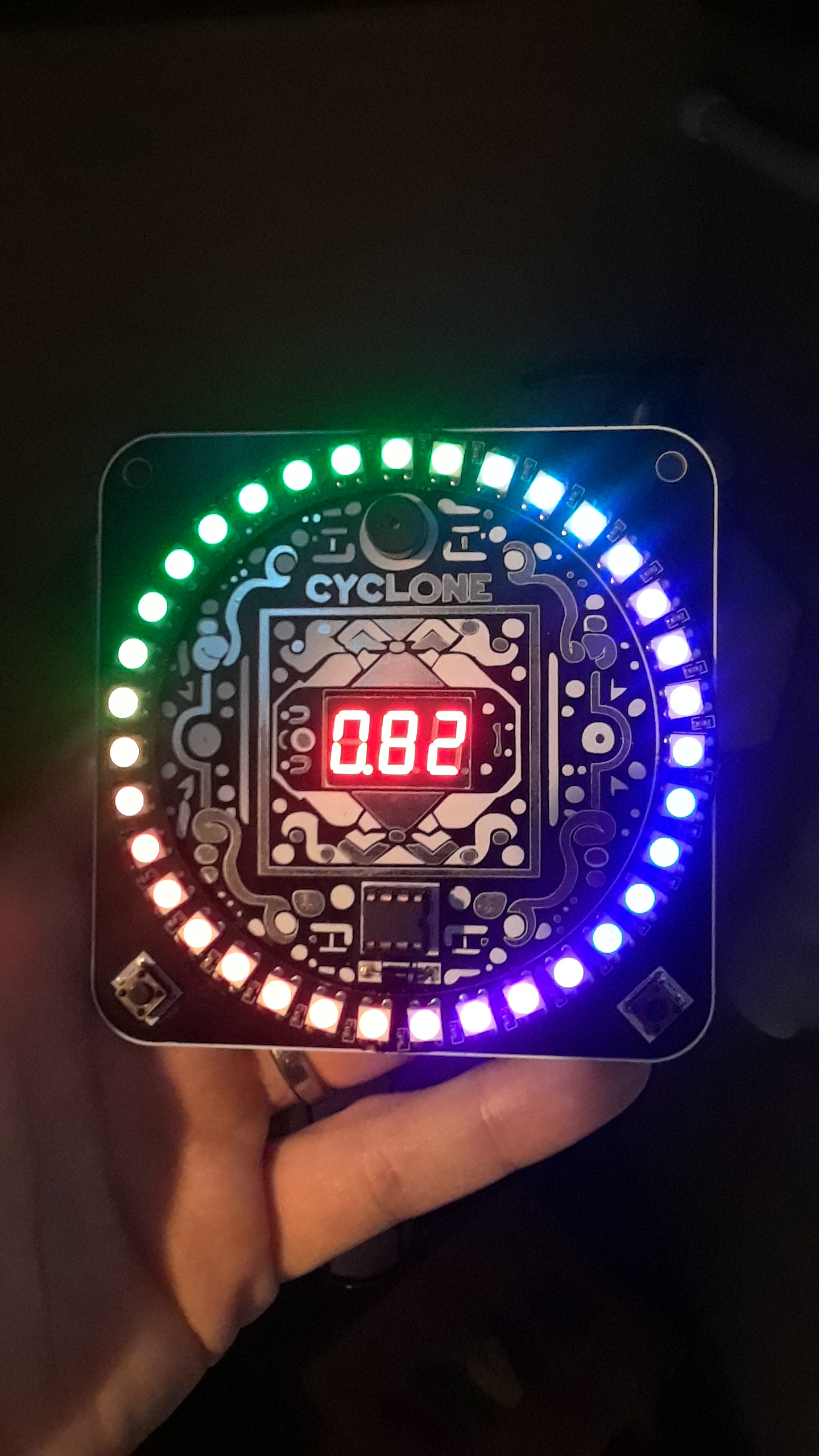
For example, the ‘Cyclone’ stop-the-light game pcb was a step too far, with my attempt to have it play music & control addressable LEDs (that’s either-or). Also the scoreboard wasn’t 100% stable since its an 5V analog meter.
The wish-you-a-merry-Christmas-tree playing ornament worked great! As did the motion sensing skull that plays Michael Meyers Halloween tune. On the other hand the number of people too young to understand that movie reference made my remaining hair turn gray.

These introductory projects made good gifts and I learned some valuable lessons. But I needed to learn how to do surface mounting in order to make anything serious. I’ve had some ideas and a specific market I want to serve; and the learn-to-solder folks ain’t it.
Step 10: SMT LETS GO!
I picked up a cheap toaster oven, a few other high temperature insulation goodies, and a Reflow Master Pro Controller and had a DIY reflow oven ready to go in 2 weekends.
A bit scary to turn on at first but it works surprisingly well! (I borrowed a thermal camera from work to double check my insulation.) It’s a great tool for prototyping & I designed a customizable 3d printable jig for holding the solder stencil to make that aspect easier.
The reflow process only takes 5 minutes, and populating a small number of surface mount components by hand is doable. Though it’s not something I’d want to do in any significant volume at home. A dozen PCBs in 1 sitting is about it.


Step 11: Get someone else to do it!
That brings me to today. In February I made my first order of fully assembled boards. All I had to do was program them. I setup a jig with spring loaded contact ‘pogo’ pins & a toggle clamp so I can process a board in about 20 seconds. The whole experience has been great! As my Mandalorian shirt says, This Is The Way.
So today I’m pleased to release a new product, a programable LED Bow Tie!
It has 3 buttons you can use to control the brightness, color, and special effects; So you can wear it as a subtle highlight or turn it up to make you the center of attention. The batteries (2x CR2450) will last through an entire event or work day and are easily replaceable.
With the optional microphone attached it enables sound reactive effects which was a fun feature to develop in 8kb of space!
Got a lot more where that came from but that’s all for now.


Update May 2024: JLC PCB Just started offering a Multi-color Silkscreen option!
https://jlcpcb.com/blog/653-multi-color-silkscreen-pcb?from=mcss

[…] Check out the process and tips in the post here. […]
LikeLiked by 1 person